Barefoot SSD Controller Technical Reference Manual
Table of Contents
- Flash Memory Configuration
- Functional Description
- Register Set
- Buffer Management and Flow Control
- SATA Operation
Permission is granted to copy, distribute and/or modify this document under the terms of the GNU Free Documentation License, Version 1.3 or any later version published by the Free Software Foundation; with no Invariant Sections, with no Front-Cover texts, and with no Back-Cover Texts. A copy of the license is included in the section entitled “GNU Free Documentation License.”
1. Flash Memory Configuration (toc)
The Jasmine platform has four flash channels. Each channel consists of a 16-bit IO bus and a number of control signals. It is recommended that you refer to the Jasmine board schematic and the NAND flash module schematic for a better understanding on flash memory configuration.
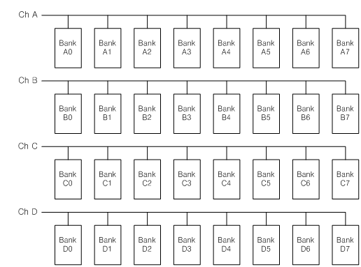
The banks are numbered as A0=0, B0=1, C0=2, D0=3, A1=4, B1=5, C1=6, D1=7, …, A7=28, B7=29, C7=30, D7=31. Up to eight banks can share a channel. Each bank has its own CE (Chip Enable) signal, output from the controller and input to the bank. Flash interface operations such as command transfer, address transfer, data transfer, and status check require IO channel to be used. The controller initiates an interface operation by activating one of the CE signals. While a CE signal is activated, the selected bank is using the IO bus to communicate with the controller. Therefore, only one CE signal can be active at a time within a channel. Since there are four channels, up to four CE signals can be active at any time. Unlike flash interface operations, flash cell operations such as programming, sensing, and erasing do not require CE signals to be active. For example, the controller can send a command that triggers a cell operation to bank A0 and then deactivate the CE signal to A0, even before the cell operation is completed by A0. While A0 is busy with the cell operation, the controller may communicate with another bank in the same channel.
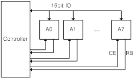
In addition to CE signal, each bank has its own RB(Ready/Busy) signal, output from the bank and input to the controller. The RB signal indicates whether the bank is busy with a cell operation. The Barefoot controller has only four, not eight, RB pins per channel. The RB output from A0 and the RB output from A4 are tied together and input to the same pin of the controller. The tie also exists between the couples A1/A5, A2/A6 and A3/A7. The other channels B, C and D are the same. Because the controller does not know whether A0 is busy or A4 is busy, the parallelism in terms of cell operation is limited to four banks at each channel.
A bank consists of two flash chips, each chip having an 8-bit interface. The controller hardware is designed so that the two chips form a virtual single chip with 16-bit interface. The data bytes are interleaved between the two chips. In most cases, the two chips receive the same command and the same address from the controller, and thus do the same operation. Only the data contents are different.

Either high chip or low chip can be optionally disabled by specifying FO_H and FO_L, respectively. Each bank has two CE signal inputs, not one, from the controller, one of which is for high chip and the other is for low chip. In most cases, FO_H nor FO_L is used and thus the two CE signals are activated and deactivated simultaneously. If you use FO_H, the high chip will ignore command/address inputs from the controller just like any other banks in the same channel will. Therefore, the data 31 4E 5A 02 C9 … in the figure will not be written if FO_H is used for a write operation. If you use FO_H for a read operation, high chip will not output any data and the controller will get unpredictable values from the chip. Note that the ECC/CRC engine has been designed without any consideration for FO_H and FO_L. If you write a data with FO_L option and then read it back with or without FO_L option, you will see an “uncorrectable data corruption” interrupt. Similarly, if you write a data not using FO_L nor FO_H option and then read it back with either FO_L or FO_H option, the same interrupt will be raised. FO_E (ECC and CRC) can be omitted in order to disable ECC/CRC engine and avoid the interrupt.
Suppose that the page size of the flash memory is 8KB. Then we find it is more convenient to regard the page size as 16KB, since two 8KB pages are read or written at the same time at two chips. The term “physical page size” refers to the native page size of the given flash memory part. The information can be found from the specification of the flash memory, published by NAND flash maker. “Virtual page size” is defined to be the basic unit of read/write operation. The high/low chip configuration makes the virtual page size to be double the physical page size. If you use FO_P option flag (two plane mode) for flash operations, the page size gets doubled again.
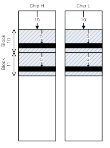
The figure shows the relationship between the physical page and the virtual page when two plane mode is used. The box filled with solid black represents a physical page. The four physical pages form one virtual page. Physical blocks #10 and #11 are paired together, because two plane mode is used. The physical pages whose offsets within the block are #5 are grouped into a single virtual page. Assuming that there are 128 pages per block, row addresses of the physical pages are calculated as 128*10 + 5 and 128*11 + 5. As for Jasmine platform, a different approach is used for row address. Since it does an automatic address translation from virtual to physical, the row address given by the firmware to the controller is a virtual row address. When two plane mode is used, the following observations can be made:
- number of virtual blocks = number of physical blocks / 4
- number of virtual pages per virtual block = number of physical pages per physical block
- the size of a virtual page = the size of a physical page * 4
Since the physical blocks #10 and #11 form a virtual block #5, the row address calculation is as follows:
row address = 128*5 + 5
When the two plane mode is not used, the following observations can be made:
- number of virtual blocks = number of physical blocks / 2
- number of virtual pages per virtual block = number of physical pages per physical block
- the size of a virtual page = the size of a physical page * 2
In this case, a physical row address and its corresponding virtual row address are identical. When the firmware requests a flash operation, it specifies a virtual address as its argument, and the controller converts it into a physical address, which is then passed to flash memory.
2. Functional Description (toc)
The firmware uses FCP (Flash Command Port) in order to initiate a flash memory operation. The FCP consists of a number of registers, which we call FCP registers. For example, if you want Bank #5 to do an erase operation, you write 5 to FCP_BANK, 0x14 (meaning erase operation) to FCP_CMD, and relevant argument values to other FCP registers. Writing to FCP registers do not trigger any hardware action. Even while the hardware is performing a flash operation, the firmware can freely read or write FCP registers in order to prepare for the next flash operation. FCP registers are not modified by the hardware and always retain the last written values. The actual hardware operation is initiated by writing an arbitrary value to FCP_ISSUE. The firmware’s action of writing a value to FCP_ISSUE is referred to as command issuing. When a command is issued, the contents of FCP registers are immediately copied to WR (Waiting Room), and the WR becomes “full.” WR is basically a queue that can hold only one entry. The firmware should not issue another command while WR is full, which will cause an undefined behavior of the controller. However, once a command has been issued, FCP can be modified by the firmware for another command even while WR is full. Your firmware will typically have a while() statement that polls until WR becomes empty immediately before issuing a new command.
The command in WR waits to be accepted by a bank. The term “accept” is defined as a bank’s action of copying WR contents to its own BSP (Bank Status Port) and then starting to perform the command. The bank becomes busy as soon as it accepts a command. A busy bank cannot accept another command. While the target bank is busy, the command keeps waiting in WR. WR becomes empty when a command is accepted. Since the contents of WR are copied to BSP upon accept, the bank relies solely on BSP contents while it is performing the command. In other words, the command being processed by a bank is kept in BSP, but not in FCP or WR.
The “Busy” status indicated through RB signal should not be confused with the “Busy” status of a bank. When a bank accepts a command, its status machine will immediately become busy. This means that the value of BSP_FSM register will immediately become non-zero. The value will become zero again upon the completion of the command. While the command is performed, flash interface operations and flash cell operations are carried out. The RB signal indicates busy status only for the cell operations. The figure shows a situation in which two banks perform FC_COL_ROW_IN_PROG. The command processing starts with a long period of interface operation followed by a long period of cell operation, and finishes with a short period of interface operation to check the cell operation result. Also note that A1 is indicated as busy even while it is doing nothing but waiting for the ownership of the channel.
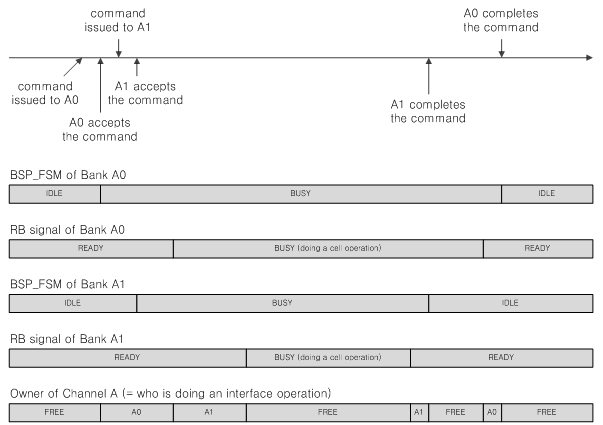
The firmware usually writes a target bank number to FCP_BANK. However, 0x3F can also be written to FCP_BANK to request Auto Select. If the target bank of the command in WR is 0x3F, the bank that becomes the most quickly idle will accept it.
Each bank has its own BSP. When a bank accepts a new command, the contents of WR are copied to the bank’s BSP, which is the only occasion of BSP register values changing.
3. Register Set (toc)
All the registers only allow 32 bit access. For example, the address of FCP_CMD is 0x60000034. When the firmware writes 0x03 to the register, the following is the correct way to do it:
*(volatile unsigned int*)0x60000034 = 0x03;
The following is an example of wrong assignments:
*(volatile unsigned short*)0x60000034 = 0x03;
*(volatile unsigned char*)0x60000034 = 0x03;
FCP_CMD
The code value of the command that the firmware wants to issue shall be written to this register. One of the following command codes can be written to this register.
- Write operations: FC_COL_ROW_IN_PROG, FC_COL_ROW_IN, FC_IN, FC_IN_PROG, FC_PROG
- Read operations: FC_COL_ROW_READ_OUT, FC_COL_ROW_READ, FC_OUT, FC_COL_OUT
- Copy operations: FC_COPYBACK, FC_MODIFY_COPYBACK
- Erase operation: FC_ERASE
- Other: FC_WAIT, FC_GENERIC, FC_GENERIC_ADDR, FC_READ_ID
FCP_BANK
The number of the bank to accept the command shall be written to this register. 0x3F can also be written to specify Auto Select. The firmware can know which bank has accepted the Auto Select command by reading WR_BANK.
FCP_OPTION
Bit flags that control optional features shall be written to this register. The effect of option flags is not global, but local to the command being issued. The following flags are defined within this register:
FO_P
- 1 = Two plane mode is used for read/write/erase operations. The controller will send an appropriate sequence of commands to the flash memory so that two plane operation is initiated. The controller will also provide a virtual row address space to the firmware. Refer to FCP_ROW for the automatic translation from virtual row address to physical row address.
- 0 = one plane mode is used for read/write/erase operations. The value in FCP_ROW register will be actually sent to high chip and low chip without any translation.
FO_E
- 1 = ECC/CRC engine is enabled for data transfer. If you enable this flag for a write operation, ECC/CRC parity bytes will be appended to each 512-byte data. If you enable this flag for a read operation, a few additional bytes after every 512-byte data will be regarded as ECC/CRC parity. This flag should not be enabled for operations that do not involve data transfer such as erase. This flag should be enabled for a data transfer between DRAM and flash. This flag may be enabled or disabled for a data transfer between SRAM and flash.
- 0 = ECC/CRC engine is disabled. It is not allowed to use two plane mode with ECC/CRC engine disabled.
FO_SCRAMBLE
- 1 = Data scrambler engine is enabled for data transfer. If you enable this flag for a write operation, the data will be randomized by the seed values in SCRAMSEED_BASE registers. If you enable this flag for a read operation the data will be descrambled by the seed values in SCRAMSEED_BASE registers.
- 0 = Data scrambler engine is disabled.
FO_L
- 1 = The CE signal to the low chip of the bank is not activated.
- 0 = The CE signal to the low chip of the bank is activated.
FO_H
- 1 = The CE signal to the high chip of the bank is not activated.
- 0 = The CE signal to the high chip of the bank is activated.
FO_B_W_DRDY
- 1 = The data transfer from the controller to a bank starts as soon as the target bank has the channel ownership. The controller assumes that the data is ready at the source buffer. This flag should only be used for write operations. This flag should not be used together with the FO_B_SATA_W flag. Either FO_B_W_DRDY or FO_B_SATA_W should be set for a write operation or the controller will stop working.
FO_B_SATA_W
- 1 = The data transfer from the controller to a bank starts when SATA_WBUF_PTR is higher than the ID of the source buffer. This flag will block the hardware operation if the host is very slow. This flag will also update the value of BM_WRITE_LIMIT when the command is completed.
FO_B_SATA_R
- 1 = The value of BM_READ_LIMIT is updated when the command is completed. Regardless of this flag, the data transfer from the target bank to the controller starts as soon as the target bank has the channel ownership. It is the firmware’s responsibility to ensure that the read buffer space does not overflow when the host is very slow.
- 0 = The value of BM_READ_LIMIT is not updated.
FCP_DMA_ADDR
The address of the source buffer of a write operation or the target buffer of a read operation shall be written to this register. This register is not used for an erase operation. For DRAM, the address shall be an integer multiple of 128. For SRAM, the address shall be an integer multiple of 4. When FO_E is not used, the actual DMA address equals FCP_DMA_ADDR value. When FO_E is used, the actual DMA address is calculated as:
Actual DMA address = FCP_DMA_ADDR + FCP_COL * 512
FCP_DMA_CNT
The number of bytes to be transferred between the controller and the bank shall be written to this register. Operations such as FC_ERASE, FC_PROG and FC_COL_ROW_READ ignore this register, since they do not involve data transfer. For a data transfer between DRAM and flash, the byte count shall be an integer multiple of 512. For a data transfer between SRAM and flash with FO_E, the byte count shall always be 512. For a data transfer between SRAM and flash without FO_E, the byte count shall be an integer multiple of 4 and shall not be greater than 512.
FCP_COL
The starting offset within a virtual page shall be written to this register. The value of FCP_COL is regarded as a sector offset if FO_E is used or as a byte offset if FO_E is not used. The actual column address that the controller sends to the target bank is calculated as:
if (FO_E == 1)
	temp = FCP_COL * (512 + PARITY_BYTES_PER_SECTOR) / 2;
else
	temp = FCP_COL;

if (FO_P == 1 && temp_is_in_the_second_plane)
	real_column_addr = temp – PHYSICAL_PAGE_SIZE;
else
	real_column_addr = temp;
Note that the division by two is due to high/low chip configuration. The controller uses the value of PG_SIZE field in FCONF_NANDCFG_2 register for the physical page size and the plane border.
FCP_ROWk_L and FCP_ROWk_H (k = 0, 1, 2, …, 31)
The virtual row address of target page shall be written to this register.
FCP_ROW0_L is for the low chip of bank #0.
FCP_ROW0_H is for the high chip of bank #0.
FCP_ROW1_L is for the low chip of bank #1.
FCP_ROW1_H is for the high chip of bank #1.
…
FCP_ROW31_L is for the low chip of bank #31.
FCP_ROW31_H is for the high chip of bank #31.
The controller converts the virtual row address to a physical row address that is sent to the flash memory. When two plane mode is used, two row addresses are sent. The following conversion rule is applied separately to low chip and to high chip:
if (FO_P is used)
    block = FCP_ROW / PAGES_PER_PBLK;
    page_offset = FCP_ROW % PAGES_PER_PBLK;
    physical_row_1 = block * 2 * PAGES_PER_PBLK + page_offset;
    physical_row_2 = real_row_1 + PAGES_PER_PBLK;
else
    physical_row = FCP_ROW;
While doing the conversion, the controller reads the BLK_SIZE field in FCONF_NANDCFG_2 register in order to determine PAGES_PER_PBLK.
Suppose that FCP_BANK is 3. Then, only FCP_ROW3_L and FCP_ROW3_H are significant and all the other FCP_ROW registers are ignored.
When Auto Select is used by setting FCP_BANK as 0x3F, the firmware cannot predict which bank will accept the command. Therefore, the firmware should ensure that every FCP_ROW register has a valid value. The values do not have to be identical. Sometimes the firmware may not want a specific bank to accept the Auto Select command. A bank will not attempt to accept an Auto Select command if high chip row address is 0xFFFFFFFF. For example, suppose that FCP_ROW5_H is 0xFFFFFFFF and FCP_BANK is 0x3F. Then, bank #3 does not accept the command even if it is idle. Although the controller was designed to support up to 32 banks, the actual configuration may be smaller and there may one or more non-existent banks. The firmware should prevent an Auto Select command from being accepted by a non-existent bank by keeping its FCP_ROW_H 0xFFFFFFFF.
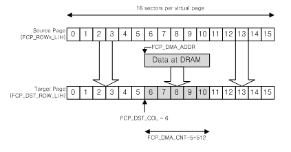
FCP_DST_COL
The firmware should write the target column address to this register when FC_COPYBACK or FC_MODIFY_COPYBACK is issued. The value of this register is ignored for any other commands. The figure shows show to set the value of FCP_DST_COL when issuing FC_MODIFY_COPYBACK. For FC_COPYBACK, it is recommended to set FCP_DST_COL as zero, since most NAND flash manuals do not explicitly specify its significance. FCP_DST_COL follows the same conversion rule as FCP_COL. Note that copy operations should always be issued with FO_E enabled and therefore FCP_DST_COL is always a sector offset. FCP_DST_COL * 512 is added to FCP_DMA_ADDR to determine the start address of DRAM-to-flash data transfer.
FCP_DST_ROW_L and FCP_DST_ROW_H
The firmware should write the virtual row address of copy operation target page. The value of this register is ignored for any command other than FC_COPYBACK or FC_MODIFY_COPYBACK.
FCP_CMD_ID
This is a 10 bit read-only register that starts from zero and counts up every time a command is issued. The value is copied together with other FCP register values from FCP to WR and finally to a BSP. You can see the value by reading BSP_k_CMD_ID.
FCP_ISSUE
The firmware should write an arbitrary value to this register in order to issue a command. The written value is not significant. The controller behavior is undefined if this register is written while WR is not empty.
WR_BANK
This is a read-only register by which the firmware can know which bank has accepted an Auto Select command. The value of this register changes whenever one the following events occur:
- When a command is issued, FCP_BANK is copied to WR_BANK.
- When a command is accepted, regardless of whether it is Auto Select or not, the number of target bank is reflected on this register.
When the firmware reads this register in order to know the target bank number of an Auto Select command, it should not issue another command before reading this register; otherwise its value will change.
WR_STAT
This is a read-only register that has two bit flags. Bit position #0 shows whether WR is full or empty. Its value is 1 while WR is full. Its value is 0 while WR is empty. Bit position #1 shows whether the controller is in pause condition. Its value is 1 while the controller is in pause condition. Refer to FCONF_PAUSE for descriptions on the pause condition.
WR_ABORT
The command in WR is aborted if an arbitrary value is written to this register. There are two ways by which WR can become empty. WR becomes empty when the command is accepted or aborted. Writing to this register while WR is empty does not have any effect.
FCONF_PAUSE
This is a configuration register by which the firmware specifies what flags of BSP_INTR registers will cause pause condition. This register has the same set of bit flags as the one in BSP_INTR registers. The controller is in pause condition while the bit-wise AND of FCONF_PAUSE and all the BSP_INTR registers is non-zero.
- If FIRQ_CORRECTED flag of this register is one, the FIRQ_CORRECTED flag in any bank’s BSP_INTR will put the controller in pause condition.
- If FIRQ_CRC_FAIL flag of this register is one, the FIRQ_CRC_FAIL flag in any bank’s BSP_INTR will put the controller in pause condition.
- If FIRQ_MISMATCH flag of this register is one, the FIRQ_MISMATCH flag in any bank’s BSP_INTR will put the controller in pause condition.
- If FIRQ_BADBLK_L flag of this register is one, the FIRQ_BADBLK_L flag in any bank’s BSP_INTR will put the controller in pause condition.
- If FIRQ_BADBLK_H flag of this register is one, the FIRQ_BADBLK_H flag in any bank’s BSP_INTR will put the controller in pause condition.
- If FIRQ_ALL_FF flag of this register is one, the FIRQ_ALL_FF flag in any bank’s BSP_INTR will put the controller in pause condition.
- If FIRQ_ECC_FAIL flag of this register is one, the FIRQ_ECC_FAIL flag in any bank’s BSP_INTR will put the controller in pause condition.
FCONF_NANDCFG_2
This is a configuration register which the firmware should set in initialization phase of the controller. The value written to this register has an immediate effect. Writing to this register while one or more banks are busy will lead to an unpredictable behavior of the controller. The register has the following fields:
BCH (0 = Reed Solomon, 1 = BCH)
- This 1 bit field specifies the type of ECC to be used.
“‘PG_SIZE”’ (0 = 2KB, 1 = 4KB, 2 = 8KB)
- This 2 bit field determines the physical page size as specified in NAND flash manual. The controller uses this information in order to determine the plane border at the center of a virtual page when two plane mode is used. It is also used to determine how many bytes to read and verify in copy operations.
“‘BLK_SIZE”’ (0 = 64, 1 = 128, 2 = 256)
- This 2 bit field determines the number of pages per block as specified in NAND flash manual. The controller uses this information in order to convert a virtual row address into a physical row address.
ECC_SIZE
- This 2 bit field determines the number of bits that can be corrected by ECC. The ECC parity size increases along with the ECC correction capability. The firmware should ensure that the space requirement does not exceed the flash memory’s actual page size. The controller does not utilize remaining space, if any.
| ECC_SIZE | Reed Solomon | BCH | ||
|---|---|---|---|---|
| Bits/Sector | ECC/CRC bytes | Bits/sector | ECC/CRC bytes | |
| 0 | 6 | 16 | 8 | 16 |
| 1 | 12 | 23 | 12 | 23 |
| 2 | 12 | 23 | 16 | 28 |
CHK_CMD (0 = 70h, 1 = 71h, 78h, F1h, 2 = given by FCONF_CHKCMD)
- This 2 bit field determines the command code the controller sends to the flash memory in order to check the result of a write or an erase operation. If this register value is 0, 70h is always used. If this register value is 1, 71h, 78h or F1h is used depending on situation. If this register value is 2, the 8 bit value of FCONF_CHKCMD is used.
CHK_CODE
- This 8 bit field is the reference value for determining whether a write or an erase operation was successful. If the status output from the flash memory does not match this value, FIRQ_BAD_BLK_H or FIRQ_BAD_BLK_L flag will be set in BSP_INTR register.
CHK_MASK
- This 8 bit field provides an option bit mask for selecting bits from the status output. The controller has the following rule:
FIRQ_BAD_BLK_L = (IO[0:7] & CHECKMASK) != CHECKCODE;
FIRQ_BAD_BLK_H = (IO[8:15] & CHECKMASK) != CHECKCODE;
FCONF_CHKCMD
This is a configuration register that holds the command code to be sent to the flash memory for status checking. Refer to CHK_CMD field of FCONF_NANDCFG_2.
FCONF_NANDCFG_1
This is a configuration register which the firmware should set in initialization phase of the controller. The value written to this register has an immediate effect. Writing to this register while one or more banks are busy will lead to an unpredictable behavior of the controller. The register has the following fields:
4. Buffer Management and Flow Control (toc)
SATA data is buffered in DRAM. You cannot use the controller’s internal SRAM for SATA data buffering. The firmware should define two non-overlapping spaces in DRAM for read buffering and for write buffering, respectively, and let the controller know the position of each. In addition, the firmware should define a third buffer space that does not overlap with the other buffers for flash copy-back operation.
Each buffer space consists of multiple buffers. The size of each buffer is identical to the virtual flash page size and is known to the controller via SATA_BUF_PAGE_SIZE register. The size of each flash copy buffer is also defined by this register.
Read Buffer
Read buffer space is an array of multiple read buffers that form a circular buffer system. The following registers are written by the firmware at the initialization phase of the controller:
- The size of each read buffer shall be written to SATA_BUF_PAGE_SIZE. Note that this information is also applied to write buffers and flash copy buffers.
- The start address of the read buffer space shall be written to SATA_RBUF_BASE. The address should be an integer multiple of SATA_BUF_PAGE_SIZE value.
- The number of buffers in the read buffer space shall be written to SATA_RBUF_SIZE.
When the firmware requests a flash read operation with FO_B_SATA_R, the address pointed to by FCP_DMA_ADDR should be a read buffer.
The controller identifies a buffer by its ID. The ID of a given buffer is calculated as:
Read buffer ID = (Address of the buffer – SATA_RBUF_BASE) / SATA_BUF_PAGE_SIZE
For the flow control of SATA read operation, there are three buffer pointers in the system.
- FTL read buffer pointer: This is a pointer in the form of global variable maintained by the firmware and the controller does not have any knowledge of it. Every time the firmware issues a flash read command with FO_B_SATA_R, the associated read buffer ID should increase by one. For example, if the buffer ID of the last command was 7, the next command should be for 8. The firmware should initialize the global variable to zero upon the system initialization phase and ensure it is always less than SATA_RBUF_SIZE.
- SATA_RBUF_PTR: This register holds the buffer ID from which the current SATA read transfer is being done. While SATA read transfer is not taking place, it points to the buffer ID of the most recent transfer. It is reset to zero upon the system initialization phase and increases by one whenever a page has been transferred by SATA. It cannot be equal to or larger than SATA_RBUF_SIZE, because of its circular nature.
- BM_READ_LIMIT: This register is maintained by the buffer manager hardware and is used by SATA hardware. The SATA read transfer can make progress only while BM_READ_LIMIT is ahead of SATA_RBUF_PTR. Upon the completion of every page transfer, the SATA hardware checks whether SATA_RBUF_PTR equals BM_READ_LIMIT. If it does, the transfer pauses until BM_READ_LIMIT increases. Usually BM_READ_LIMIT increases by one upon the completion of a flash read with FO_B_SATA_R. However, in case of out-of-order completion, it does not increase or increases by more than one upon such an event. For example, if a read operation from bank #9 to read buffer #2 finishes later than another read operation from bank #15 to read buffer #3, the earlier completion of the latter does not increase BM_READ_LIMIT and the later completion of the former increases BM_READ_LIMIT by two.
The firmware is responsible for the flow control in case SATA speed is slower than the firmware and flash memory. When the firmware issues a flash read command with FO_B_SATA_R, it should make sure the associated read buffer ID is not equal to the current value of BM_READ_LIMIT or SATA_RBUF_PTR. By defining the number of read buffers to be larger than the number of banks, the need to care about BM_READ_LIMIT is removed. However, the firmware should still have a waiting loop for SATA_RBUF_PTR before issuing a command.
Write Buffer
Write buffer space is an array of multiple write buffers that form a circular buffer system. The following registers are written by the firmware at the initialization phase of the controller:
- The size of each write buffer shall be written to SATA_BUF_PAGE_SIZE. Note that this information is also applied to read buffers and flash copy buffers.
- The start address of the write buffer space shall be written to SATA_WBUF_BASE. The address should be an integer multiple of SATA_BUF_PAGE_SIZE value.
- The number of buffers in the write buffer space shall be written to SATA_WBUF_SIZE.
When the firmware requests a flash write operation with FO_B_SATA_W, the address pointed to by FCP_DMA_ADDR should be a write buffer.
The controller identifies a buffer by its ID. The ID of a given buffer is calculated as:
Write buffer ID = (Address of the buffer – SATA_WBUF_BASE) / SATA_BUF_PAGE_SIZE
Note that a buffer ID is not unique across read buffer space, write buffer space and copy buffer space. The first buffer of write buffer space has the ID value of zero, the same as the first buffer of read buffer space.
For the flow control of SATA write operation, there are three buffer pointers in the system.
- FTL write buffer pointer: This is a pointer in the form of global variable maintained by the firmware and the controller does not have any knowledge of it. Every time the firmware issues a flash write command with FO_B_SATA_W, the associated write buffer ID should increase by one. For example, if the buffer ID of the last command was 7, the next command should be for 8. The firmware should initialize the global variable to zero upon the system initialization phase and ensure it is always less than SATA_WBUF_SIZE.
- SATA_WBUF_PTR: This register holds the buffer ID to which the current SATA write transfer is being done. Since the buffer system is circular, it is guaranteed that the buffers behind SATA_WBUF_PTR have valid data. It is reset to zero upon the system initialization phase and increases by one whenever a page has been transferred by SATA. It cannot be equal to or larger than SATA_WBUF_SIZE, because of its circular nature.
- BM_WRITE_LIMIT: This register is maintained by the buffer manager hardware and used by SATA hardware. The SATA write transfer can make progress only while BM_WRITE_LIMIT is ahead of SATA_WBUF_PTR. Upon the completion of every page transfer, the SATA hardware checks whether SATA_WBUF_PTR equals BM_WRITE_LIMIT. If it does, the transfer is pauses until BM_WRITE_LIMIT increases. Usually BM_WRITE_LIMIT increases by one upon the completion of a flash write with FO_B_SATA_W. However, in case of out-of-order completion, it does not increase or increases by more than one upon such an event. For example, if a write operation from bank #9 to write buffer #2 finishes later than another write operation from bank #15 to write buffer #3, the earlier completion of the latter does not increase BM_WRITE_LIMIT and the later completion of the former increases BM_WRITE_LIMIT by two.
The firmware is not responsible for the flow control of write stream. Therefore, it is allowed for the firmware to issue a command with FO_B_SATA_W, even before the data is ready. The firmware does not have to wait for SATA to DRAM transfer completion before issuing the command. For every buffer, the hardware will wait for the completion of SATA to DRAM transfer before starting DRAM to flash transfer. Suppose that a bank has accepted the command for which buffer ID 7 is given. The data transfer from DRAM to the bank will only start when SATA_WBUF_PTR is 8 or higher.
The number of write buffers (i.e. SATA_WBUF_SIZE) should be large enough to ensure that no two banks accept write commands with the same buffer ID.
Flash Copy Buffer
Flash copy buffer space is an array of multiple buffers for flash copy-back operation. Copying data from a flash page to another involves the following steps if performed without utilizing copy-back feature:
- A page is read and the data is transferred from flash to DRAM. During this step, any bit error is corrected by ECC and the DRAM contains the resultant data. Typically FC_COL_ROW_READ_OUT is used for this step.
- The data is transferred back to flash and programmed to a new page. Typically FC_COL_ROW_IN_PROG is used for this step.
Using copy-back feature, the steps are as follows:
- A page is read, by read-for-copy-back command, and the data is transferred from flash to DRAM. During this step, any bit error is corrected by ECC.
- One or more corrected sectors are transferred back to flash. If there has been no ECC correction in the first step, this second step is not performed.
- The data is programmed to a new page.
FC_COPYBACK covers all three steps, where a flash copy buffer is used during the data transfer to/from flash. Each bank exclusively owns its flash copy buffer and the size of each buffer is defined by SATA_BUF_PAGE_SIZE. The firmware has to define a dedicated space in DRAM where there are 32 buffers, and let the hardware know its start address through FCONF_CPBDMABASE register.
Misalignment
There are three types of buffers: read buffer, write buffer and flash copy buffer. Regardless of its type, the size of each buffer equals to SATA_BUF_PAGE_SIZE which is the size of virtual page size. However, the basic unit of data transfer to/from buffers is not a page but a sector (i.e. 512 bytes) and therefore a transfer may not align to buffer boundary. For a SATA read transfer, the start address is determined by the following rule:
DRAM address of buffer = SATA_RBUF_BASE + SATA_RBUF_PTR * SATA_BUF_PAGE_SIZE
Sector offset = SATA_SECT_OFFSET % (SATA_BUF_PAGE_SIZE / 512)
Transfer start address = (DRAM address of buffer) + (Sector offset) * 512
The start address of SATA write transfer is determined by the following rule:
DRAM address of buffer = SATA_WBUF_BASE + SATA_WBUF_PTR * SATA_BUF_PAGE_SIZE
Sector offset = SATA_SECT_OFFSET % (SATA_BUF_PAGE_SIZE / 512)
Transfer start address = (DRAM address of buffer) + (Sector offset) * 512
For a flash read/write transfer with FO_E, the start address is determined by the following rule:
Transfer start address = FCP_DMA_ADDR + FCP_COL * 512
For FC_MODIFY_COPYBACK, the start address of DRAM-to-flash transfer is determined by the following rule:
Transfer start address = FCP_DMA_ADDR + FCP_DST_COL * 512
Overriding
Usually the firmware does not need to manipulate BM_READ_LIMIT and BM_WRITE_LIMIT, because they are automatically updated upon completion of flash operations. However, there may be special occasions that those pointers are required to be updated by the firmware.
For example, suppose that the firmware wants to discard (i.e. not write to flash memory) the user data in buffer ID 7. Updating FTL write buffer pointer from 6 to 8 is necessary but not sufficient, because the buffer manager hardware is waiting for the completion message for 7 from any bank. Since the firmware has not issued a write command for 7, BM_WRITE_LIMIT will be stuck at 6 forever. In this case, BM_STACK_WRSET and BM_STACK_RESET registers are used for the forced update of BM_WRITE_LIMIT. The firmware writes 8 to BM_STACK_WRSET and then writes 1 BM_STACK_RESET. Writing 1 to the bit 0 of BM_STACK_RESET causes the value of BM_STACK_WRSET to be copied to BM_WRITE_LIMIT. Care must be taken to ensure that there is not race condition between the forced update and the automatic update.
Similarly, writing an arbitrary buffer ID to BM_STACK_RDSET and writing 1 to the bit 1 of BM_STACK_RESET causes a forced update of BM_READ_LIMIT. BM_READ_LIMIT and BM_WRITE_LIMIT can be updated at the same time by writing 0x03 to BM_STACK_RESET.
5. SATA Operation (toc)
SATA operation is driven by interrupts. The following types of interrupts are defined for SATA.
CMD_RECV
When a non-FPDMA command is received, CMD_RECV is raised. Note that NCQ_CMD_RECV will be raised for FPDMA commands. SATA_FIS_H2D registers are read by the firmware for command parsing. Depending on whether it is a read/write command or not, the firmware should process it in a different manner.
Upon a reception of a read/write command, its parameters such as LBA and sector count should be inserted into SATA Event Queue. LBA and sector count should be written to SATA_LBA register and SATA_SECT_CNT register, respectively. Note that writing to those registers does not initiate any hardware action. When 1 is written to SATA_INSERT_EQ_W register, the contents of SATA_LBA and SATA_SECT_CNT are recognized as write command parameters and inserted into SATA Event Queue. Writing 1 to SATA_INSERT_EQ_R register treats them as read command parameters. SATA Event Queue is typically monitored by the firmware’s top level infinite loop which removes an entry from the queue and calls FTL read function or write function accordingly. Using the hardware implemented SATA Event Queue is optional. If your firmware has another command queue, CMD_RECV interrupt handler does not have to insert an entry into SATA Event Queue.
After inserting the read/write command into the queue, the interrupt handler has to initiate a SATA transfer. Note that CMD_RECV interrupt can occur asynchronously with respect to FTL operation. For example, 5th write command can be received and raise an interrupt while FTL is handling 2nd write command, in which case three commands will be queued. Therefore, the interrupt handler should immediately initiate the SATA transfer for write commands in order to maximize the write speed. As for read commands, initiating the SATA transfer by the interrupt handler will not improve the read speed, compared to initiating the SATA transfer by FTL, because the actual transfer will start when flash read operation is finished. In order for the firmware to initiate SATA transfer, it has to set up parameters such as SATA_XFER_BYTES and SATA_SECT_OFFSET registers. Writing to SATA_CTRL_2 register initiates the SATA transfer. The actual transfer is subject to flow control by BM_READ_LIMIT and BM_WRITE_LIMIT.
When CMD_RECV interrupt occurs for a command other than read or write, the firmware should not insert it into the SATA Event Queue. Examples include IDENTIFY_DEVICE, SMART and FLUSH.
NCQ_CMD_RECV
FPDMA commands raise NCQ_CMD_RECV interrupt. Note that FPDMA commands can be received even before the transfer of previous command starts, if NCQ size is configured to be larger than one. When an FPDMA command is received, the hardware automatically inserts it into the NCQ at the same time it raises NCQ_CMD_RECV interrupt. The NCQ is a data structure kept in SRAM whose address is pointed to by SATA_NCQ_BASE register. The firmware has to define the data structure and write its SRAM address to SATA_NCQ_BASE while initializing the system.
OPERATION_OK
When the SATA transfer initiated by the firmware is completed successfully, OPERATOIN_OK interrupt is raised. This is an indication that a SATA command has been processed in protocol point of view. Note that it is not related to the completion of FTL operation. The hardware automatically sends register FIS D2H to host at the same time it raises this interrupt.
OPERATION_ERR
A CRC error in data FIS will lead to OPERATION_ERR instead of OPERATION_OK. The firmware should manually send register FIS D2H to host in order to report the unsuccessful termination of the command.